




Blitz India Business
NEW DELHI: Three of the twelve facilities approved under the India Semiconductor Mission are operational, against approvals of more than $21 billion. Read as a scorecard that looks like slippage. Read against how long a fab actually takes to build, it is roughly on time — and the number that matters is not the count.
The mission’s approvals now exceed $21 billion across twelve commercial facilities, of which three are running. The flagship remains Dholera in Gujarat: a ₹91,000-crore line sized for 50,000 wafers a month at the 28-nanometre node, with trial production targeted for December. Twenty-eight nanometres is not the frontier — leading-edge logic is several generations finer — and that is a deliberate choice rather than a shortfall. The 28nm and larger nodes are where the automotive controllers, power management chips, display drivers and industrial microcontrollers are made: high-volume, long-lived, less capital-punishing parts, and precisely the categories India currently imports in quantity.
The unit of progress: a fab’s honest milestones are yield and qualification, not the ribbon-cutting that precedes them by a year or more.
A fab is not finished when it opens. It is finished when a customer accepts the third batch. That gap is where semiconductor ambitions are usually settled.
At a Glance
• Approved facilities: twelve commercial units under the India Semiconductor Mission
• Operational: three
• Total approvals: more than $21 billion
• Dholera: a ₹91,000-crore fab sized for 50,000 wafers a month
• Node: 28 nanometres — the mature-node segment used in automotive, power, display and industrial chips
• Trial production: targeted for December
• The real milestone: qualified yield accepted by a paying customer, typically well after first silicon
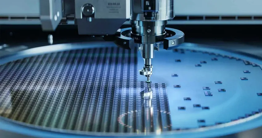
The structural point that gets lost in the count is what a semiconductor fab actually is. It is a building whose contents cost several times the building, whose water must be purer than anything in the municipal system, whose power supply cannot flicker, and whose equipment is supplied by a handful of firms with multi-year order books. From approval to first wafer is typically three to five years for a greenfield site anywhere in the world, and from first wafer to qualified, customer-accepted yield is another meaningful stretch. Judged against that clock, three operational facilities within the mission’s life is not slow. What would be genuinely slow is an ecosystem that never forms around them — and that is the metric worth tracking instead.
That ecosystem is the whole game, and it is where India’s advantage is real. The country already supplies a very large share of the world’s semiconductor design engineering; what it has lacked is everything on either side of the wafer — specialty gases and chemicals, photomasks, substrates, precision components, and the assembly, testing, marking and packaging step that is far less capital-intensive than fabrication and far more employment-intensive. Building that layer is slower than announcing a fab and considerably more durable, because it serves every fab, including the ones built elsewhere. The right way to read the scoreboard, then, is to stop counting facilities. Count qualified suppliers, count packaging lines, count process engineers trained and retained. Those are the numbers that decide whether India has a semiconductor industry in 2035 or a set of very expensive buildings.