




Blitz India Business
A Tata–PSMC fab at Dholera now roughly 50% built, first silicon targeted for late 2026, and an ASML lithography pact secured in May — India’s semiconductor mission is moving decisively from paper to plant.
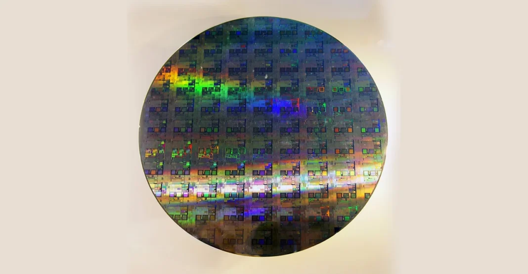
Tata Electronics, partnered with Taiwan’s Powerchip (PSMC), is building an ~$11 billion (₹91,000 crore) Dholera fab designed for about 50,000 wafers a month at 28nm–110nm, targeting roughly 3 billion chips a year. A May 16 MoU with Netherlands-based ASML, signed in The Hague, secures the DUV lithography that front-end fabrication requires; a full fabrication unit is expected by 2028.
The investment case now rests on execution — talent, supplier ecosystems and utilities are the variables that decide returns, not policy intent.
By the Numbers
- Dholera fab: ~$11 bn (₹91,000 cr), ~50,000 wafers/month
- Node: 28nm–110nm; ~3 bn chips/year
- Progress: ~50% built; first silicon late 2026
- Enabler: Tata–ASML DUV MoU, The Hague, May 2026
For component and materials suppliers, the pipeline signals a multi-year domestic demand curve — gases, chemicals, testing and packaging — where India can build supplier depth around each fab. Analysts caution that headline timelines and scale claims still need to be met on the ground.
The constructive priority is de-risking execution: specialised talent pipelines, reliable power and water, and incentives that pull the vendor ecosystem into the country.